The Snapdragon 888 vs The Exynos 2100: Cortex-X1 & 5nm - Who Does It Better?
by Andrei Frumusanu on February 8, 2021 3:00 AM EST- Posted in
- Mobile
- Samsung
- Qualcomm
- Smartphones
- SoCs
- Snapdragon 888
- Exynos 2100
5nm / 5LPE: What do we know?
Starting off with the biggest new change of this generation, both the Snapdragon 888 and the Exynos 2100 are manufactured on Samsung’s new 5nm process node, which is the biggest unknown in today’s comparison.
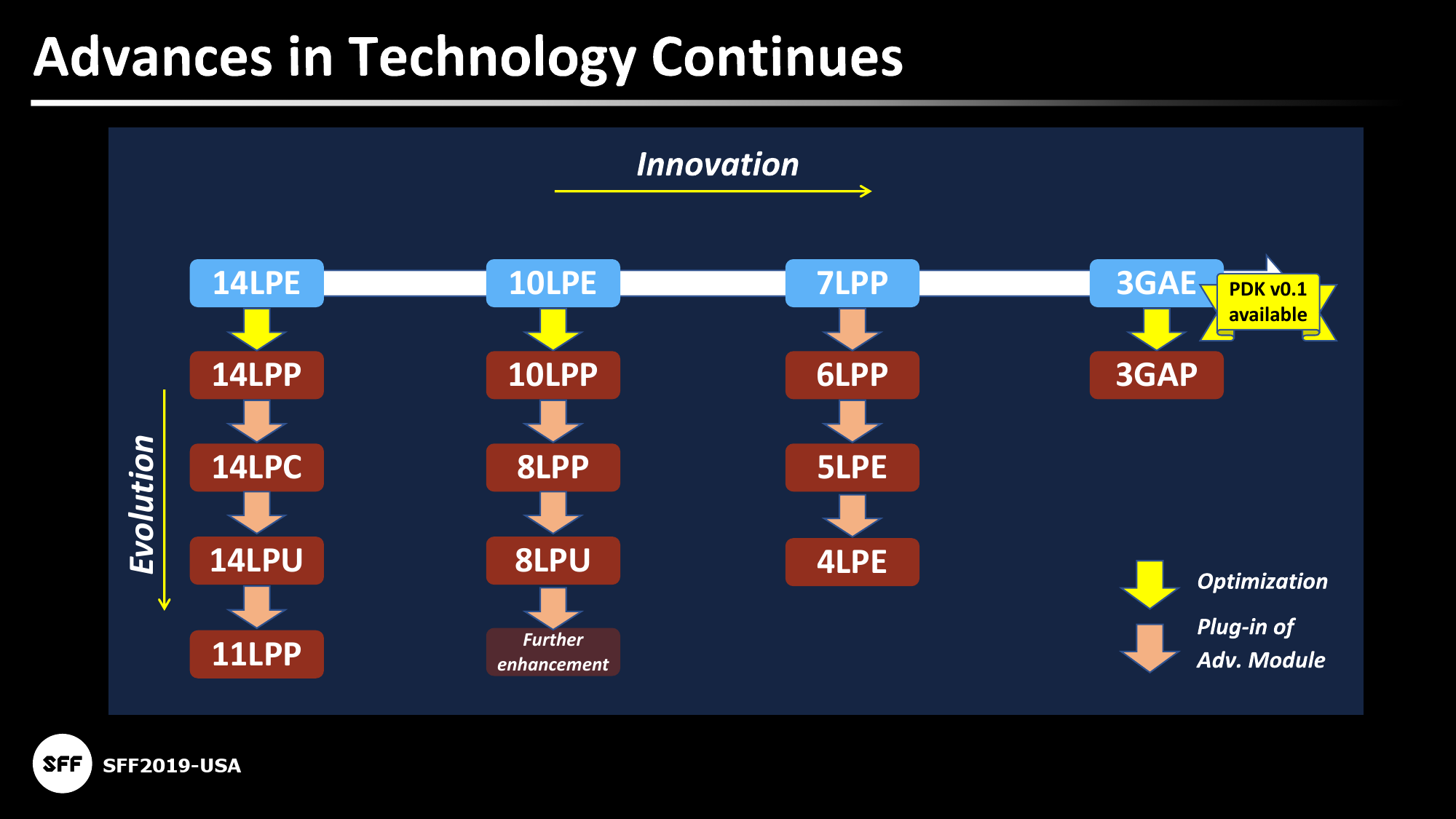
What’s important to remember is that although Samsung calls this node 5nm, its design and characteristics are more similar to that of their 7nm node. Key new characteristics of the new node here are the reintroduction of single diffusion breaks (SDB) on an EUV process node, as well as slight changes in the cell libraries of the process.
| Advertised PPA Improvements of New Process Technologies Data announced by companies during conference calls, press briefings and in press releases |
||||||
| 7LPP vs 10LPE |
6LPP vs 7LPP |
5LPE vs 7LPP |
3GAE vs 7LPP |
|||
| Power | 50% | lower | 20% | 50% | ||
| Performance | 20% | ? | 10% | 35% | ||
| Area Reduction | 40% | ~9% | <20% | 40% | ||
Per Samsung’s own numbers, the foundry claims that 5LPE is either 20% lower power than 7LPP, or 10% more performance. These are actually quite important figures to put into context, particularly when we’re comparing designs which are manufactured on TSMC’s process nodes.
In least year’s review of the Galaxy S20 series and the Exynos 990 and Snapdragon 865 SoCs, an important data-point that put things into context was Qualcomm’s Snapdragon 765 SoC which was also manufactured on Samsung’s 7LPP node, and featuring Cortex-A76 cores. In that comparison we saw that The Exynos 990 and the Snapdragon 765’s A76 cores behaves very similarly in terms of power consumption, however they fell behind TSMC-based Cortex-A76 cores by anywhere from 20% to 30%.
In that context, Samsung’s 5LPE process node improving power by 20% would mean they’d only be catching up with TSMC’s 7nm nodes.
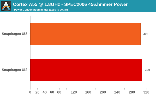
An interesting comparison to make – and probably one of the rare ones we’re actually able to achieve today, is the comparison between the Cortex-A55 cores inside of both the Snapdragon 865 and the new Snapdragon 888. Both SoCs feature the same IP cores, clock them at the same 1.8GHz frequency, and both feature the same amount of L2 cache, with their only real difference being their process nodes.
Using SPEC’s 456.hmmer – because it’s a workload that primarily resides in the lower cache hierarchies and thus, we avoid any impact of the possibly different memory subsystem, we can see that both SoCs’ power consumption indeed is almost identical, with performance also being identical with a score of 6.84 versus 6.81 in favour of the new Snapdragon 888.
So at least at first glance, our theory that Samsung’s 5LPE merely just catches up with the power consumption and power efficiency of TSMC’s N7/N7P nodes seems to be valid – at least at these frequencies.

Further interesting data is the voltage curves of the CPUs on the Exynos 2100. I’ve extracted the frequency voltages tables of both my devices, a regular S21 and an S21 Ultra, with the above curves being the better binned chip inside of the smaller S21.
Generationally, Samsung seems to have been able to greatly reduce voltages this generation. On the Cortex-A55 cores, the cores now only require 800mV at 2GHz whilst the Exynos 990 last year in our review unit they required over 1050mV. Similarly, although the comparison isn’t apples-to-apples, the Cortex-A78 cores at 2.5GHz only require 862mV, while the Cortex-A76 cores of the previous generation required also 1050mV.
What’s also very interesting to see is the voltage curves of the Cortex-X1 cores versus the Cortex-A78 cores: they’re both nigh identical to each other, which actually lines up with Arm’s claims that the new X1 cores have the same frequency capabilities as the A78 cores, only being larger and increasing their power consumption linearly in relation to their frequency.
Samsung’s frequency tables indicate that they had been testing the A55 up to 2.6GHz, and the X1 and A78 cores up to 3.2GHz – however voltages here are quite higher and it’s also likely SLSI wouldn’t have been able to achieve similar chip yields.
Unfortunately, I wasn’t able to extract data from my Snapdragon 888 S21 Ultra, so I can’t tell exactly where it falls in terms of voltages compared to the Exynos 2100. One thing I can confirm as being quite different between the two SoCs is that Samsung does actually give the Exynos 2100’s Cortex-X1 core its own dedicated voltage rail and PMIC regulator, while the Snapdragon 888 shares the same voltage rail across the X1 and A78 cores. In theory, that could mean that in more mixed-thread workloads, the Exynos has the opportunity to be more power efficiency than the Snapdragon 888.
Generally, the one thing I want people to take away here is that although Samsung calls this their 5nm node, it’s quite certain that it will not perform the same as TSMC’s 5nm node. Usually we don’t care about density all too much, however performance and power efficiency are critical aspects that effect the silicon and the end-products’ experiences.


123 Comments
View All Comments
serendip - Monday, February 8, 2021 - link
I'm interested in what this means for the SD8cx successor. A 30% increase from using one or two X1 cores would be great, I'm using the SQ2 chip and that's fast enough for typical office tasks. That's still not enough to get within striking range of the M1 or even A14. What the heck is in those Firestorms that makes them so fast?On memory subsystems, what are Qualcomm and Samsung doing wrong compared to Apple and HiSilicon? The M1's memory bandwidth is astonishingly high but that's from using custom parts. HiSilicon is doing a great job using standard ARM interconnects.
Agreed on the stupidly high GPU clocking. The SQ2 has a beefy GPU that performs well but it can get hot even in a large tablet form factor. It's time to stop the marketing departments from forcing engineers to chase pointless metrics.
ikjadoon - Monday, February 8, 2021 - link
>What the heck is in those Firestorms that makes them so fast?A trifecta that I share with people because this question comes up so often.
Technical Part 1: https://www.anandtech.com/show/16226/apple-silicon...
Technical Part 2: https://www.anandtech.com/show/16252/mac-mini-appl...
Consumer + Approachable: https://www.youtube.com/watch?v=3SG5e4z-Ygg
Technical Background + More Approachable: https://www.youtube.com/watch?v=cAjarAgf0nI
As Upscaled wrote, "It's not magic. It's good design." And why don't AMD / Intel have these same good designs? The videos above give thorough answers. For example, the last link explains why everyone cares Firestorm (A14) and Lightning (A13) have an 8-wide decode, which is one of many major "better designs" versus competing Arm & x86 CPUs.
ikjadoon - Monday, February 8, 2021 - link
Uh, wait. Delete. I definitely skipped too much of that one. What on Earth is he going on about 1T vs 1C?~~ Consumer + Approachable: https://www.youtube.com/watch?v=3SG5e4z-Ygg ~~
Wow, I'm a little stunned at how bad this Upscaled video is. The Dev Doc + AnandTech are much more reliable.
Nicon0s - Monday, February 8, 2021 - link
LoL, Engadget.He keeps saying multithreading when he means SMT or Hyperthreading(Intel's version of SMT).
ikjadoon - Monday, February 8, 2021 - link
Yes! Never mind 1T / 1C have shown negligence IPC differences in general computing. 1% at best. Please go test an i5-8600K vs an i7-8700K: one has SMT, one does not. Terrible to see the WCCFTech disinformation cycle reach a mainstream audience so quickly.https://www.anandtech.com/show/16261/investigating...
And then he, out of left field, throws up a Cinebench multi-core score: "See? Intel and Apple are actually very close to each other." But, his comparison was the 4+4 M1 vs an 8C Intel...
I wish I could edit comments. I give up on consumer YouTube videos; I saw his earlier interview with RISC's founders and it seemed halfway decent. I'm a fool.
Archer_Legend - Tuesday, February 9, 2021 - link
Don't be offended but I think that what you posted is completely bs.First of all you are comparing arm64 cpus and x86 cpus, second the arm 64 cores used by apple are very arguably faster than the x86 cores of for example a ryzen cpu.
The second thing which I would want to point out is that about the widht of the pipeline, it is not that apple is a genious or intel and amd are stupid: the x86 architecture was built to have a narrowish pipeline and do more cycles in fact the width of the pipeline in intel and amd cpus is as wide as it gets.
Arm arch on the other end lets you use a wider pipeline, however saying using a narrower or wider pipeline is better or not is pointless because performance comes down to how you organise the cpu around that specific pipeline so....
leledumbo - Monday, February 8, 2021 - link
> What the heck is in those Firestorms that makes them so fast?The same thing since A9 again (CMIIW): super wide decoder + super big cache. Apple isn't stingy when it comes to die size and Apple SoCs are always bigger than Snapdragon on the same generation and process node. 4mm^2 difference is huge when we're talking at nm level. What's weird, Exynos is even bigger but can't match these two. No idea what Samsung put there.
Santoval - Tuesday, February 9, 2021 - link
"What's weird, Exynos is even bigger but can't match these two. No idea what Samsung put there."This is probably due to TSMC having a *far* denser 5nm process node compared to Samsung's process 5nm node. Per the article below TSMC's 5nm node tops at 173 million transistors per mm^2 while Samsung's 5nm node reaches only 126.5 MTr/mm^2 (i.e. barely denser than TSMC's second gen 7nm+ node) due to much more, er, "conservative" design choices (Samsung basically just switched from DDB cells in 7nm to SDB cells; the article explains what that means).
What is often not clear is that the quoted transistor densities of each process node are always the *maximum* transistor densities, not the actual transistor densities used to fab a die. For instance Intel have three different 10nm node variants with three different densities, a low, mid and high density variant (ranging I believe from ~55 million to ~100 million transistors per mm^2). The last one is the only one that has been widely reported, the other two were intended for the tech savvy press and audience.
Each Intel 10nm die has a mix of all three libraries, but each design is (obviously) *fixed* with a precise mix of the three. The desktop parts always have a higher percentage of low density cells because these need to clock higher, and vice versa for the mobile parts. Mobile phones are efficiency focused, so their SoCs have the highest percentage of the highest density variant of each process node that is possible (without hindering performance too much).
That is an additional reason their clocks top at ~3 GHz. Since the two SoCs of the article are both mobile SoCs of an almost identical design we can assume a roughly equivalent percentage of the highest density cells each process node maxes out at. Thus, if all else was being equal (including the same iGPU) Samsung's SoC would have a roughly ~27% larger die than TSMC's SoC. That must be the main reason Samsung kept the cache sizes of the X1 and the A55 cores low.
Santoval - Tuesday, February 9, 2021 - link
p.s. Sorry, I forgot the link to the article :https://semiwiki.com/semiconductor-manufacturers/s...
Santoval - Tuesday, February 9, 2021 - link
p.s.2 I just noticed that the Snapdragon 888 is also fabbed with Samsung's 5nm node. While that rendered the comparison between the two SoCs in my above comment moot the other things I pointed out might have some "academic" value regarding process nodes (I have no away to delete the comment anyway..).