Semiconductors
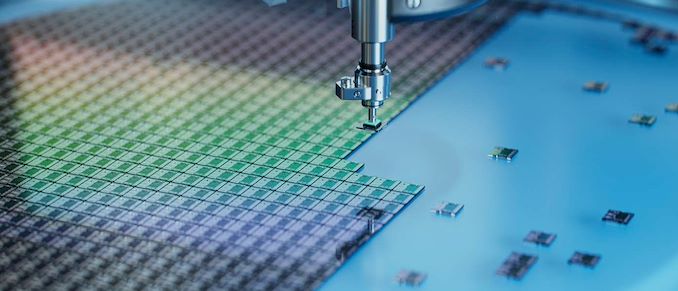
One of the core challenges that Rapidus will face when it kicks off volume production of chips on its 2nm-class process technology in 2027 is lining up customers. With Intel, Samsung, and TSMC all slated to offer their own 2nm-class nodes by that time, Rapidus will need some kind of advantage to attract customers away from its more established rivals. To that end, the company thinks they've found their edge: fully automated packaging that will allow for shorter chip lead times than manned packaging operations. In an interview with Nikkei, Rapidus' president, Atsuyoshi Koike, outlined the company's vision to use advanced packaging as a competitive edge for the new fab. The Hokkaido facility, which is currently under construction and is expecting to begin equipment installation...
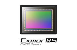
Sony to Build New Fab to Boost CMOS Sensor Output
Sony this week has revealed that the company will be building a new semiconductor fab to boost output of its CMOS sensors, as part of a broader effort to...
16 by Anton Shilov on 11/1/2019
GlobalFoundries and TSMC Sign Broad Cross-Licensing Agreement, Dismiss Lawsuits
GlobalFoundries and TSMC have announced this afternoon that they have signed a broad cross-licensing agreement, ending all of their ongoing legal disputes. Under the terms of the deal, the...
27 by Anton Shilov on 10/28/2019
Intel Files Antitrust Suit Against SoftBank-Controlled Firm Over Patent Aggregation
Intel this week filed an lawsuit against Fortress Investment Group, a patent assertion entity controlled by SoftBank. Responding to a series of patent infringement lawsuits that Fortress has brought...
21 by Anton Shilov on 10/23/2019
TSMC: 5nm on Track for Q2 2020 HVM, Will Ramp Faster Than 7nm
TSMC’s 5 nm (N5) manufacturing technology is projected to provide significant benefits when it comes to performance, power, and area scaling, which is why the contract maker of semiconductors...
27 by Anton Shilov on 10/23/2019
New Tools Simplify Development of 2.5D Multi-Die 7nm Designs at Samsung Foundry
Advanced packaging technologies simplify production and increase performance of highly-complex multi-die SoCs as the semiconductor industry is looking at chiplet approach as an alternative to large dies that take...
5 by Anton Shilov on 10/22/2019
TSMC Radically Boosts CapEx to Expand Production Capacities, To Reach $14B For 2019
Forecasting strong demand for its 5 nm and 7 nm class process technologies in the coming years, TSMC has announced that it's increasing its capital expenditure for 2019 by...
18 by Anton Shilov on 10/18/2019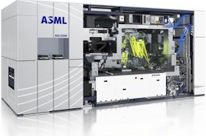
EUV Demand is Up: EUV Device Manufacturer ASML Beats Sales Estimates
Between the smartphone revolution, cloud computing, and the Internet of Things, the demand for cutting-edge chips has never been higher. And if you have any doubts about that, then...
46 by Anton Shilov on 10/16/2019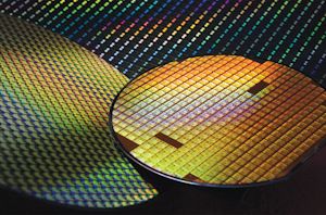
Samsung & TSMC Develop 8nm & 7nm Automotive-Grade Nodes
As vehicles are getting ‘smarter’ and gaining autopilot capabilities, it is easy to predict that the demand for higher-performing and more complex automotive SoCs will be growing rapidly in...
29 by Anton Shilov on 10/14/2019
New Tools & IP Accelerate Development of 5nm Arm ‘Hercules’ SoCs
Arm, Synopsys, and Samsung Foundry have developed a set of optimized tools and IP that will enable chip designers to build next-generation SoCs based on Arm’s Hercules processor cores...
9 by Anton Shilov on 10/10/2019
TSMC: N7+ EUV Process Technology in High Volume, 6nm (N6) Coming Soon
TSMC announced on Monday that its customers have started shipping products based on chips made by TSMC using its N7+ (2nd Generation 7 nm with EUV) process technology that...
27 by Anton Shilov on 10/8/2019
GlobalFoundries Mulls IPO Plans for 2022
After a decade of being a privately-held contract maker of semiconductors, GlobalFoundries has revealed that it's mulling going public in 2022. The move will help GF’s current owners to...
9 by Anton Shilov on 10/2/2019
TSMC Counter-sues GlobalFoundries: Accuses US Fab of Infringing Patents Across Numerous Process Nodes
In a not-unexpected move, TSMC late on Monday filed a lawsuit against GlobalFoundries, its pure-play foundry rival, accusing the manufacturer of patent infringment. In the suit, a response to...
24 by Anton Shilov on 10/1/2019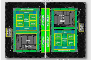
Arm & TSMC Showcase 7nm Chiplet, Eight A72 at 4GHz on CoWoS Interposer
Arm and TSMC this week unveiled their jointly developed proof-of-concept chip that combines two quad-core Cortex-72-based 7 nm chiplets on TSMC’s Chip-on-Wafer-on-Substrate (CoWoS) interposer. The two chips are connected...
26 by Anton Shilov on 9/27/2019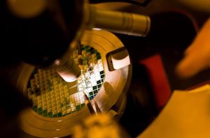
GlobalFoundries Unveils 12LP+ Technology: Massive Performance & Power Improvements
GlobalFoundries has introduced its 12LP+ fabrication process that relies on the groundwork set by its 14LPP and 12LP technologies and provides significant improvements when it comes to performance, power...
41 by Anton Shilov on 9/25/2019
TSMC Responds to Lawsuit by GlobalFoundries: Allegations Are Baseless
TSMC has responded to GlobalFoundries accusations of patents infringements. The world’s largest foundry said that it would defend itself in courts and that it considered allegations as baseless. The...
62 by Anton Shilov on 8/27/2019
GlobalFoundries Sues TSMC Over Patent Infringement; Apple, Qualcomm, Others Named Defendants
GlobalFoundries has filed a lawsuit against TSMC and its clients in the USA and Germany alleging the world’s largest contract maker of semiconductors of infringing 16 of its patents...
97 by Anton Shilov on 8/26/2019
SMIC: 14nm FinFET in Risk Production; China's First FinFET Line To Contribute Revenue by Late 2019
SMIC, the largest contract maker of semiconductors in China, announced this month that it would start commercial production of chips using its 14 nm FinFET manufacturing technology by the...
53 by Anton Shilov on 8/16/2019
GlobalFoundries Sells Off Photomask Assets to Toppan
Following its decision to focus on specialized process technologies last August, GlobalFoundries has been consolidating its assets as well as selling off businesses and facilities that are not essential...
20 by Anton Shilov on 8/15/2019
Samsung’s Aggressive EUV Plans: 6nm Production in H2, 5nm & 4nm On Track
Samsung Foundry formally started to produce chips using its 7LPP (7 nm low power plus) fabrication process last October and has not slowdown development of its manufacturing technologies since...
42 by Anton Shilov on 7/31/2019
TSMC Announces Performance-Enhanced 7nm & 5nm Process Technologies
TSMC has quietly introduced a performance-enhanced version of its 7 nm DUV (N7) and 5 nm EUV (N5) manufacturing process. The company’s N7P and N5P technologies are designed for...
36 by Anton Shilov on 7/30/2019


