GlobalFoundries' 22FDX with MRAM is Ready
by Anton Shilov on February 27, 2020 8:00 AM EST- Posted in
- Semiconductors
- GlobalFoundries
- 22nm
- Everspin
- 22FDX
- eMRAM
GlobalFoundries on Thursday said that it had completed development of its 22FDX (22 nm FD-SOI) technology with embedded magnetoresistive non-volatile memory (eMRAM). The technology can be used for a variety of applications, including automotive, industrial-grade MCU, and Internet-of-Things (IOT). Several clients of GlobalFoundries are ready to tape out their first 22FDX chips with eMRAM this year.
eMRAM provides a number of advantages when compared to eFlash (which is widely used today) for chips that need relatively high-capacity onboard storage, including higher performance and endurance, but want it all in a single silicon die. MRAM does not involve electric charges or current flows, instead, it uses magnetic storage elements and relies on reading the magnetic anisotropy (orientation) of two ferromagnetic films separated by a thin barrier. The method does not require an erase cycle before writing data, which means additional performance. Furthermore, MRAM can be produced using modern process technologies and has a very high endurance. The technology has some downsides, which will be eventually addressed by fabrication processes that use ReRAM, but GlobalFoundries and Samsung Foundry see a huge potential in in MRAM for the vast majority of applications.

GlobalFoundries’s says that test chips produced using its 22FDX with eMRAM process technology have demonstrated a 100,000-cycle endurance and a 10-year data retention across the -40°C to 125°C operating temperatures with ECC-off mode. Furthermore, the company’s eMRAM test product can pass standard reliability test, including LTOL (168 hours), HTOL (500 hours), and 5x solder reflows with failure rate < 1 ppm. In addition, GlobalFoundries has addressed concerns about magnetic immunity (of a product that relies on magnetic storage elements). The company says that its test 40 Mb product demonstrated a stand-by magnetic immunity of ~ 600 oersted at 105°C for 10 years (which means no read failures), whereas its active-mode magnetic immunity was ~500 oersted.
GlobalFoundries offers silicon-validated MRAM macros featuring capacities from 4 Mb to 48 Mb that can be used for various designs. At present, the technology has been qualified for AEC-Q100 Grade 2 designs with a -40°C to 105°C temperature range. Next year, the company will offer a version of the process qualified for AEC-Q100 Grade 1 temperatures (-40°C to 125°C).
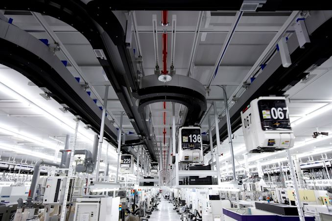
GlobalFoundries produces chips using its 22FDX technology at its 300-mm Fab 1 in Dresden, Germany. The same production facility will handle production of devices made using the company’s 22FDX with eMRAM.
Mike Hogan, senior vice president and general manager of automotive and industrial multi-market at GlobalFoundries said the following:
“We continue our commitment to differentiate our FDX platform with robust, feature rich solutions that allow our clients to build innovative products for high performance and low power applications. Our differentiated eMRAM, deployed on the industry’s most advanced FDX platform, delivers a unique combination of high performance RF, low power logic and integrated power management in an easy-to-integrate eMRAM solution that enables our clients to deliver a new generation of ultra-low power MCUs and connected IoT applications.”
Related Reading
- Samsung Ships First Commercial Embedded MRAM (eMRAM) Product
- MRAM Developer Day, GlobalFoundries Keynote Live Blog
- Everspin Begins Production of 1Gb STT-MRAM
- GlobalFoundries Teams Up with Singapore University for ReRAM Project
Source: GlobalFoundries


7 Comments
View All Comments
drexnx - Thursday, February 27, 2020 - link
FD-SOI lives!and apparently so does GloFo R&D!
psychobriggsy - Thursday, February 27, 2020 - link
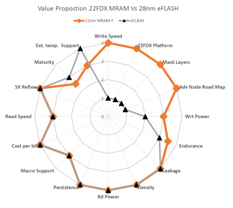
I like that one of the spider diagram benefits of 22nm MRAM versus 28nm eFlash is 22nm support (4 points for MRAM, 0 for eFlash).Also they couldn't bear to give MRAM 2 points for maturity, so it's the only score with a .5 for no appreciable reason.
But it does look like a good technology, especially going forward to smaller nodes, where eFlash will be very difficult to scale to.
boeush - Thursday, February 27, 2020 - link
Hard to judge just how quantitative - rather than qualitative - those scores really are. That said, they also have it at 3.5 on "Endurance".I can see 22 nm support as a defensible benefit if it enables the rest of the chip to also be on 22 nm (as opposed to 28 nm)...
Also they never gave a 0 score to anything; fit some reason their minimum is 1 even though 0 is available on the diagram...
What do you expect. It's marketing, not engineering.
Fataliity - Thursday, February 27, 2020 - link
Is their 14 FDX out yet? The power consumption and cost advantages would make a good use for an IO die in my opinion.spaceship9876 - Thursday, February 27, 2020 - link
I think you mean 12FDX.Dragonstongue - Thursday, February 27, 2020 - link
I want an SSD made with this stuff, for reasonable cost ^.^I can see how this would be a massive boon vs the "bust" IMHO that QDC/QLC whatever you want to call it IS...i.e much less P/E cycles much higher chance of failure, not really massive jump (as promised sic.) for pretty much same price as "tried and true" TLC or MLC designs.
this probably will not likely be used as such, but still, overheat or "too cold" not an issue, want to put your drive in "cold storage" for an extended period of time, not a problem, likely backed by 5-7 years warranty, not a problem.
would be kick A** (^.^)
boozed - Monday, March 16, 2020 - link
"MRAM does not involve electric charges or current flows"So how does it read and write?