Marvell Unveils its Comprehensive Custom ASIC Offering
by Andrei Frumusanu on July 27, 2020 12:00 PM EST- Posted in
- Semiconductors
- Networking
- Marvell
- Enterprise
- Infrastructure
Last week Marvell had updated us with an overview of the company’s new more extensive and comprehensive custom ASIC offerings, detailing the company’s design abilities for customers who are seeking to deploy differentiated products.

People traditionally familiar with Marvell will know the company from their products in the processor and baseband chipset spaces, having also a large footprint in the storage device controller space as well as other networking space. Most recently we’ve reported on the company’s booming business in the 5G infrastructure processors with the Octeon TX2 and Octeon Fusion products.
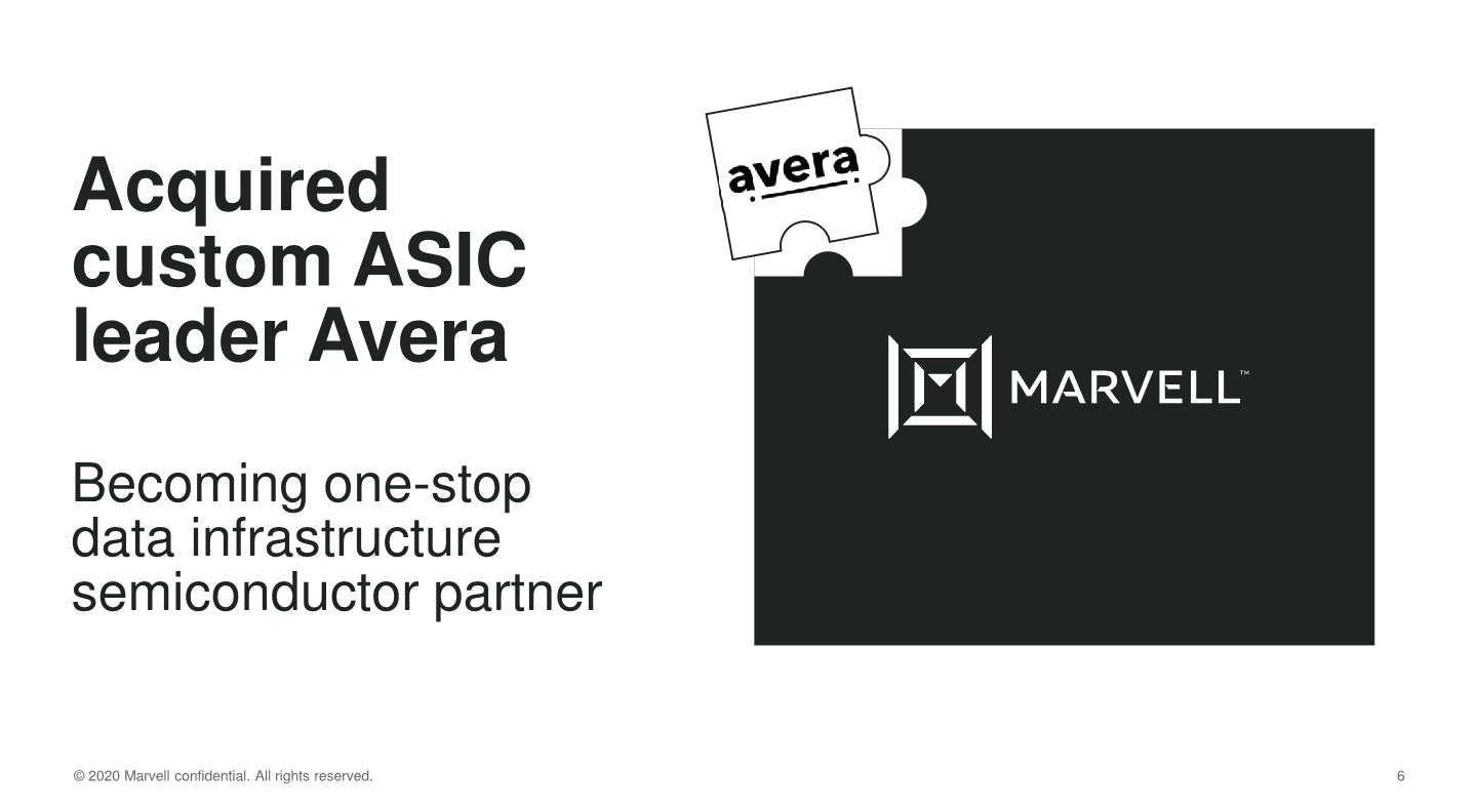
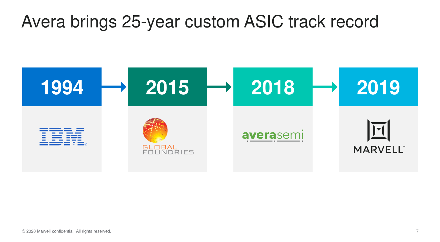
Last year, Marvell had acquired Avera Semiconductor, which was prior to 2018 a custom ASIC design division of Globalfoundries and prior to that a longer and well-known history as part of IBM. With GlobalFoundries having exited the leading-edge process node manufacturing business, the division had been spun off as AveraSemi, and had a brief stint as a independent company before Marvell quickly showed interest in purchasing the lot.
We briefly covered the topic of Marvell being able to develop custom variations of their Octeon processor line back a few months ago, and the team and resources which enable the company to achieve this are the ex-Avera people which have joined forces with Marvell’s own teams and extensive IP portfolio.
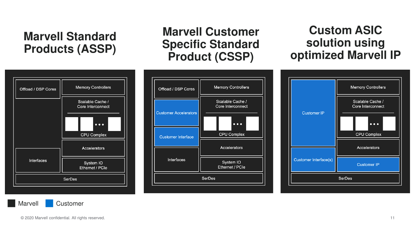
In essence, what is happening here is Marvell is offering a unique business model in terms of offering customised product hardware design that are either developed by Marvell themselves, or integrate third-party IP by a given product.
Customer specific products would be something akin to how AMD currently operates its semi-custom business in that they take requests and design requirements from a customer and design a specific product based on IP that the company also separately maintains for its own “vanilla” products. Marvell’s offering here in terms of custom products also leverages their IP portfolio, allowing designs opportunities with a large level of flexibility.
Going further, and which is seemingly unique (or very rare), is the ability for Marvell to integrate custom customer IP blocks, which opens up a whole new business model for companies who wish to have custom silicon for specific tasks, but do not have the resources or the design ability to create a whole silicon design themselves.
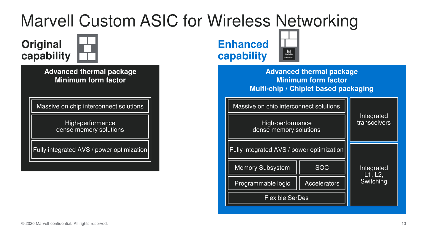
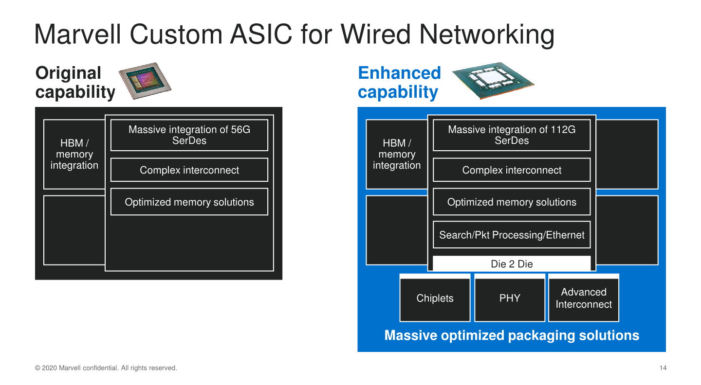
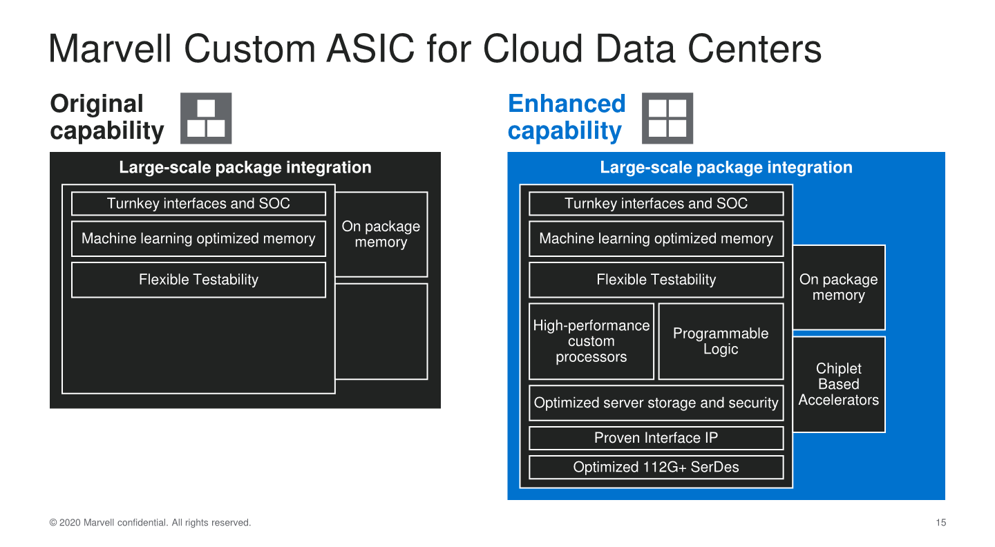
Marvell here showcases a vast variety of solution opportunities, with the Avera custom ASIC team showcasing the vastly expanded opportunities and abilities that have been enhanced by their integration into Marvell’s existing business, adding Marvell’s expertise in memory subsystems, programmable logic, accelerator IP, processing units and a very large scale of IP including unique opportunities such as custom CPU microarchitectures (They also offer Arm IP cores). Least to say, the capabilities have seen a huge leap in terms of breadth and quality of IP.
The custom ASIC offering would be extremely interesting in areas of wireless or wired networking designs, or even custom data-centre silicon.
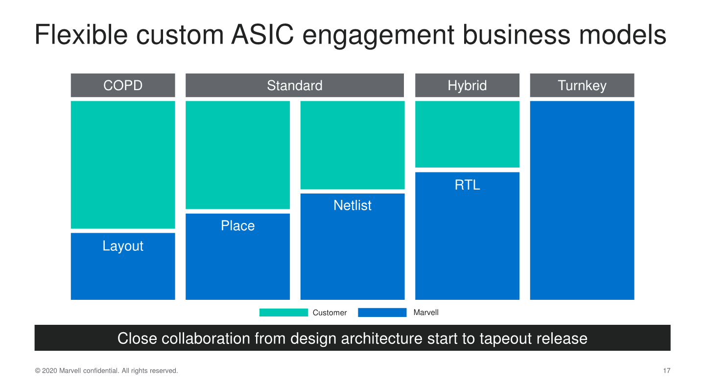
There are various levels of engagement for customers based on their needs and resources. This gradient ranges from either fully custom turnkey designs by Marvell, down to various intermediate models where the design work is shared between the customer and the Marvell team. A customer for example could have their own IP design, but would hand it over to Marvell for synthesis and physical design. A more advanced customer who might have more design resources on their side might simply just share a hard macro of their IP block with Marvell left with doing the layout on the chip.

In essence, Marvell’s new custom ASIC division would act as a design-house for a wide range of customers who are looking for custom silicon without having to invest resources of brining up a design team themselves. Imagine this being newcomers, or maybe even larger companies who want a more unique product and don’t have the design bandwidth to develop it.
Design bandwidth of the team is probably the biggest advantage for Marvell, as the scale of the operations is what allows it to be profitable and justify itself in the first place. In smaller companies with a more serial design approach one doesn’t necessarily have the ability to do multiple projects at the same time. The custom ASIC team here would be able to work on several parallel projects in tandem, with a pipeline design approach of various teams such as RTL, verification, physical design and validations teams working all on different projects. The division has a quoted decades old track-record of working on 14 leading-edge process nodes and having produced over 2000 custom designs.
With leading-edge process node designs ballooning in terms of costs and the ever-increasing barrier to entry, it seems a sensible decision to be able to out-source your chip design to a design house which has such versatile resources at hand.
In terms of process nodes and foundries, the company’s 14nm offerings are obviously tied to Globalfoundries given the close history the team has had with the foundry in the past. Current and next-generation designs are developed for TSMC’s 7 and 5nm nodes (Although the company didn’t directly name TSMC, the insinuation was obvious).
Related Reading:
- Marvell’s ThunderX3 Server Team Loses VP/GM and Lead Architect
- Marvell Announces ThunderX3: 96 Cores & 384 Thread 3rd Gen Arm Server Processor
- Marvell Announces OCTEON Fusion and OCTEON TX2 5G Infrastructure Processors
- Marvell at FMS 2019: NVMe Over Fabrics Controllers, AI On SSD
- Marvell Announces Client SSD Controllers With PCIe Gen4
- Marvell to Acquire Avera Semiconductor from GlobalFoundries


6 Comments
View All Comments
jjthejetphan - Monday, July 27, 2020 - link
I'm excited to see this play out. I think there's a real market in the area between "I'm stretching the limits of FPGA" and "I'm not big enough to justify custom ASIC".Arsenica - Monday, July 27, 2020 - link
"the company’s 14nm offerings are obviously tied to Globalfoundries given the close history the team has had with the foundry in the past. Current and next-generation designs are developed for TSMC’s 7 and 5nm nodes *Although the company didn’t directly name TSMC, the insinuation was obvious)"If you assume that their 14nm offerings are tied to GloFo you can apply the same logic and conclude that <10nm offerings are tied to Samsung "given the close history the team has had with the foundry in the past".
anonomouse - Monday, July 27, 2020 - link
Their 14nm custom ASIC briefs explicitly call out GlobalFoundries.hehatemeXX - Monday, July 27, 2020 - link
In this world it's about software leveraging the hardware. NM conversations are useful, but also silly to compare 14nm & 7nm. These chips are paid for in software creation. The difference between $50 a chip and $65 a chip are empty when the end customer pays $2-25,000 for a card.ksec - Thursday, July 30, 2020 - link
Not a single word on the new logo and branding? I thought this signals Marvell is now very different to what they were known for.5G solution from Samsung is a relatively tiny market, I wonder if the custom ASIC solution will bring Nokia or Ericsson on board.
Crazyeyeskillah - Monday, August 17, 2020 - link
Marvell's custom Asic division is one of only a few that has shipped working Tensor cores.