Hot Chips 2020 Live Blog: NVIDIA A100 Performance (5:00pm PT)
by Dr. Ian Cutress on August 17, 2020 7:50 PM EST
07:58PM EDT - First talk of the GPU session is from NVIDIA, on the A100 performance and the Ampere architecture
08:00PM EDT - Open question if they'll talk about Ampere for environments other than HPC, but this session is also about 'Gaming', so you never know
08:02PM EDT - Intel's John Sell, ex-Microsoft, is the chair for the session
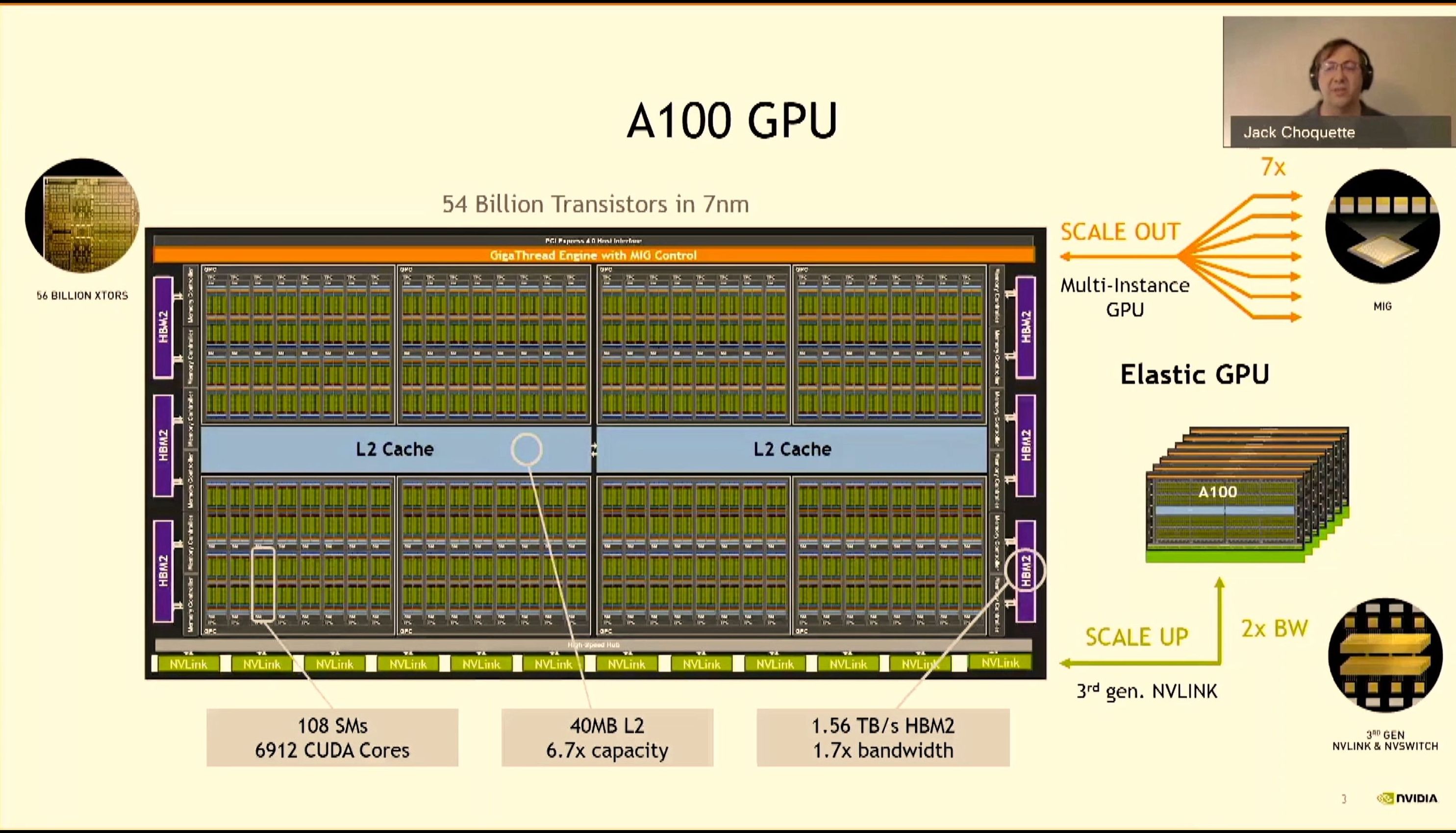
08:03PM EDT - Jack Choquette from NV
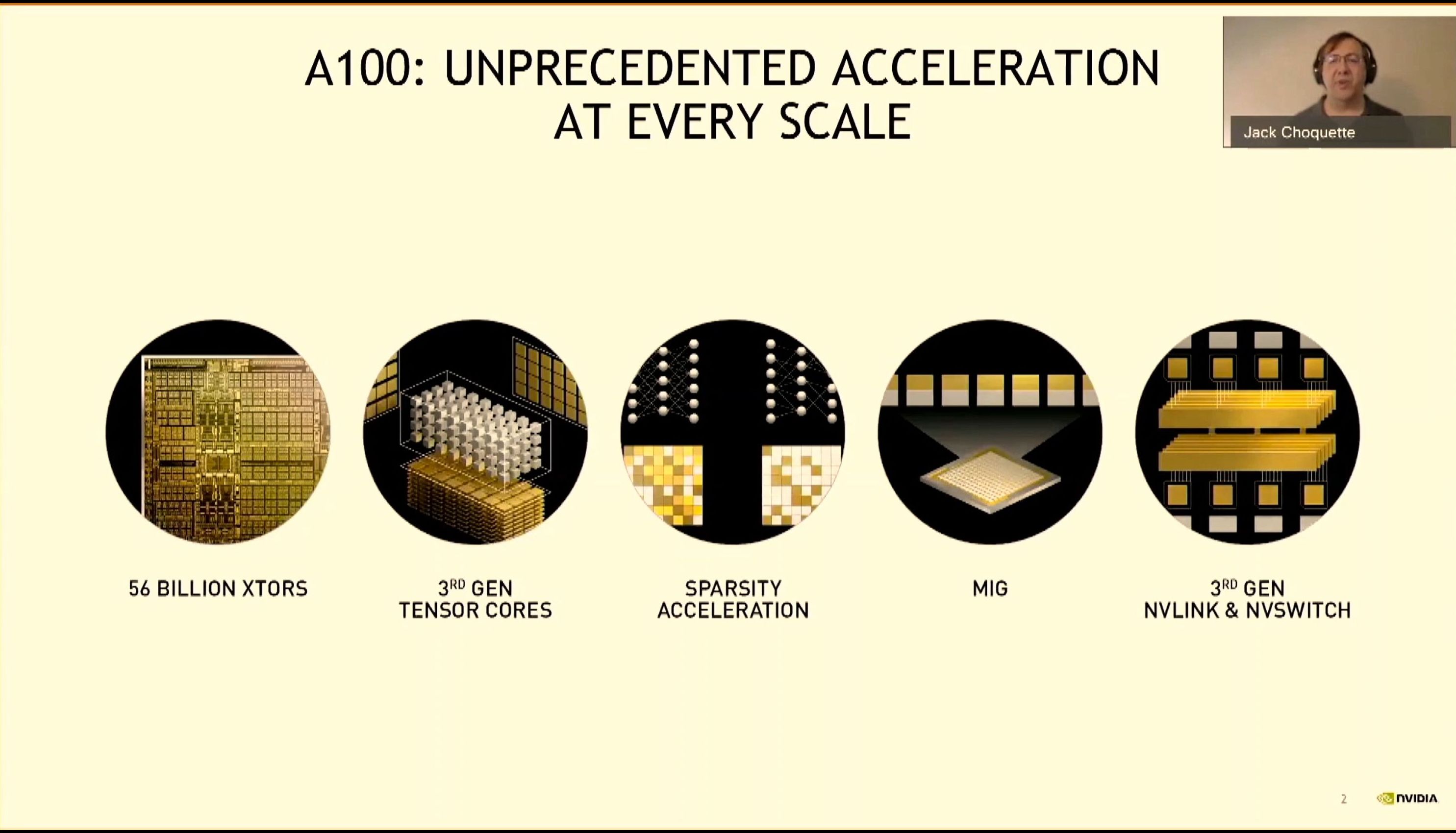
08:03PM EDT - A100: 54-56B transistors
08:03PM EDT - 6912 CUDA Cores

08:04PM EDT - 1.6 TB/sec HBM2 bandwidth
08:04PM EDT - Elastic GPU, scale out with 3rd Gen NVLink
08:04PM EDT - 2x-7x improvements over V100 overall
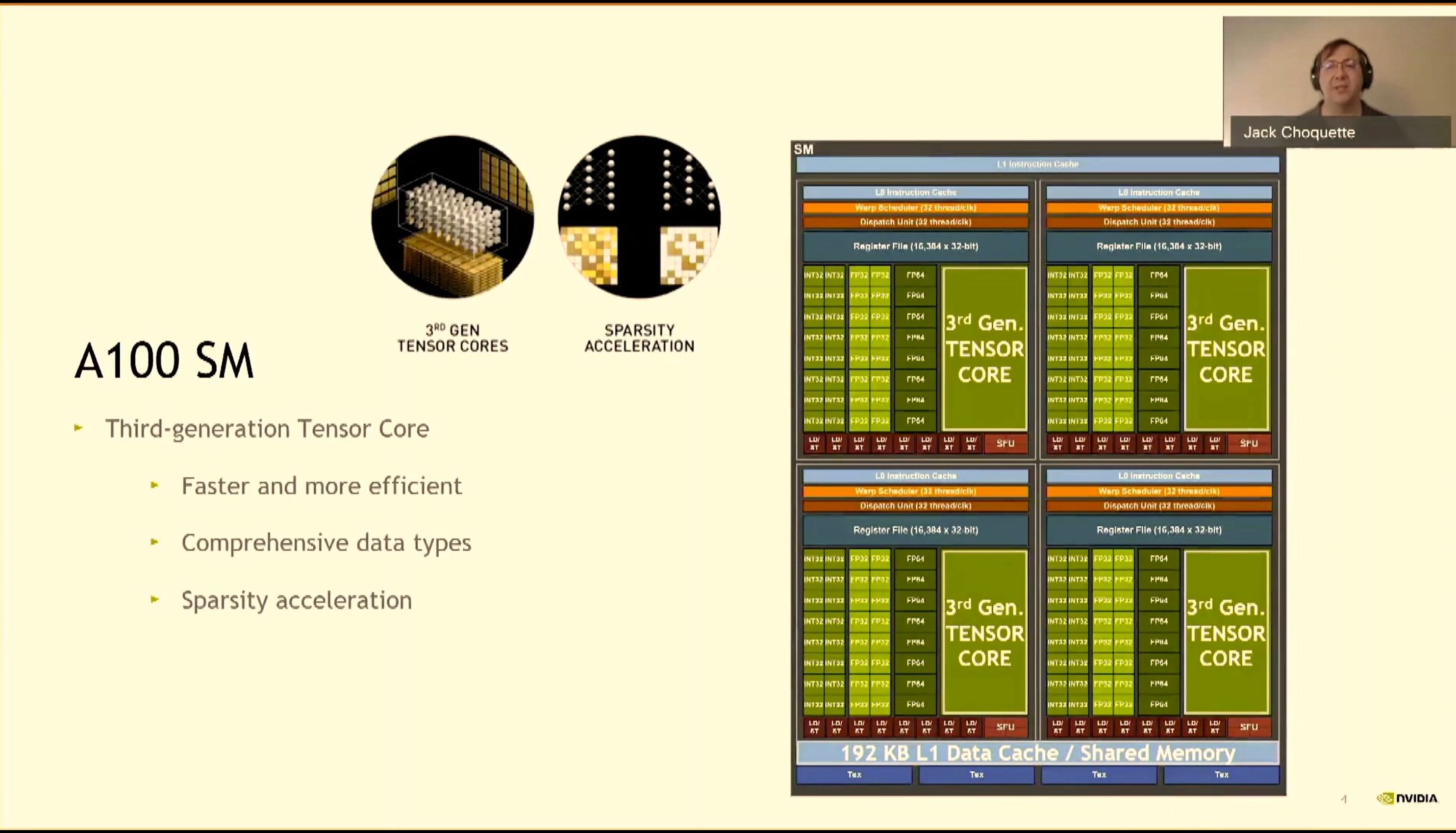
08:05PM EDT - Next-Gen Tensor Core
08:05PM EDT - More efficient, improves perf with sparsity
08:05PM EDT - Increased L1, async data movement


08:05PM EDT - Performance uplift against V100
08:06PM EDT - IEEE for FP64 MatMul
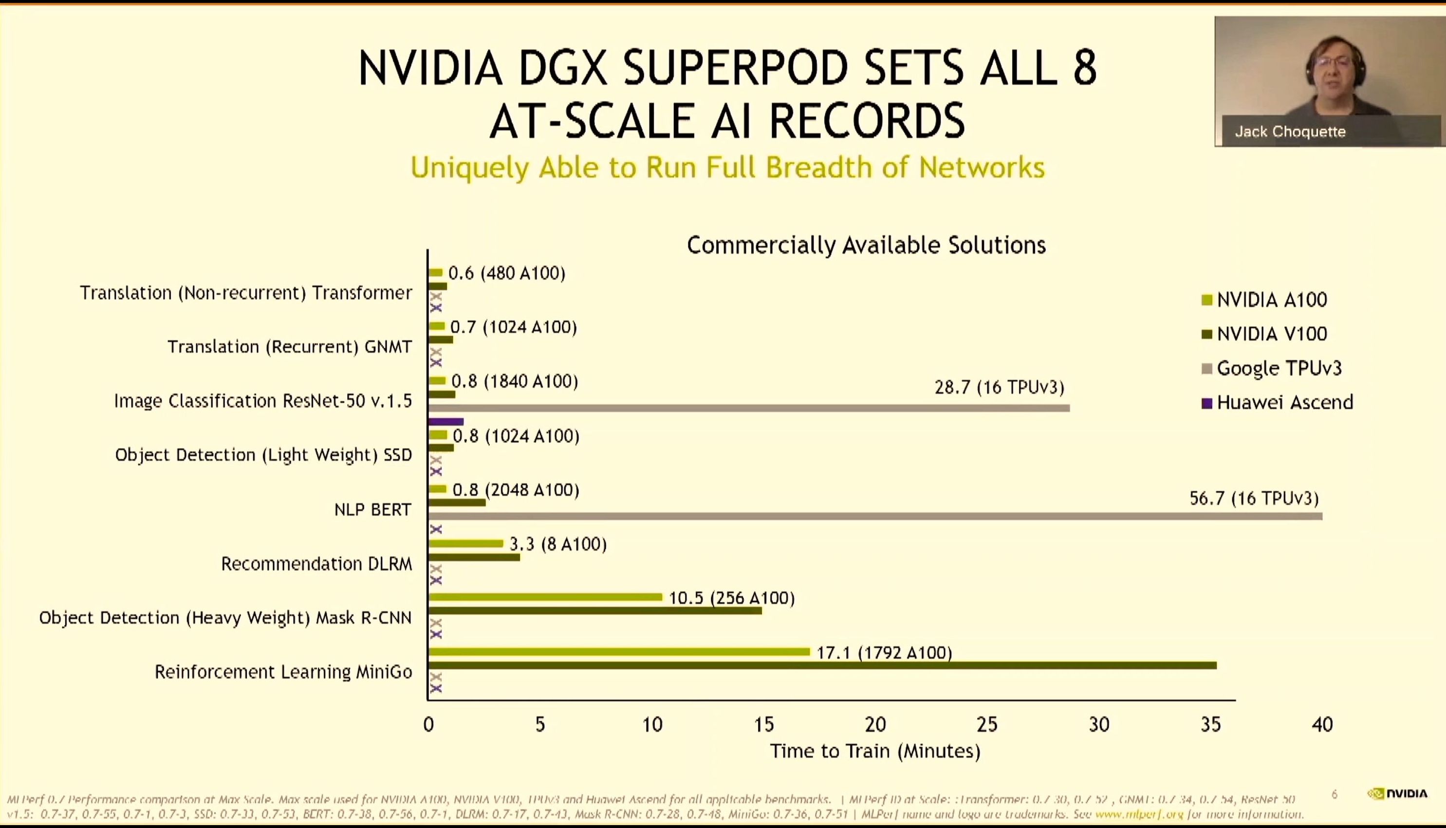
08:06PM EDT - Records on MLPerf with A100 Pods
08:06PM EDT - A100 dominates in per-chip performance as well
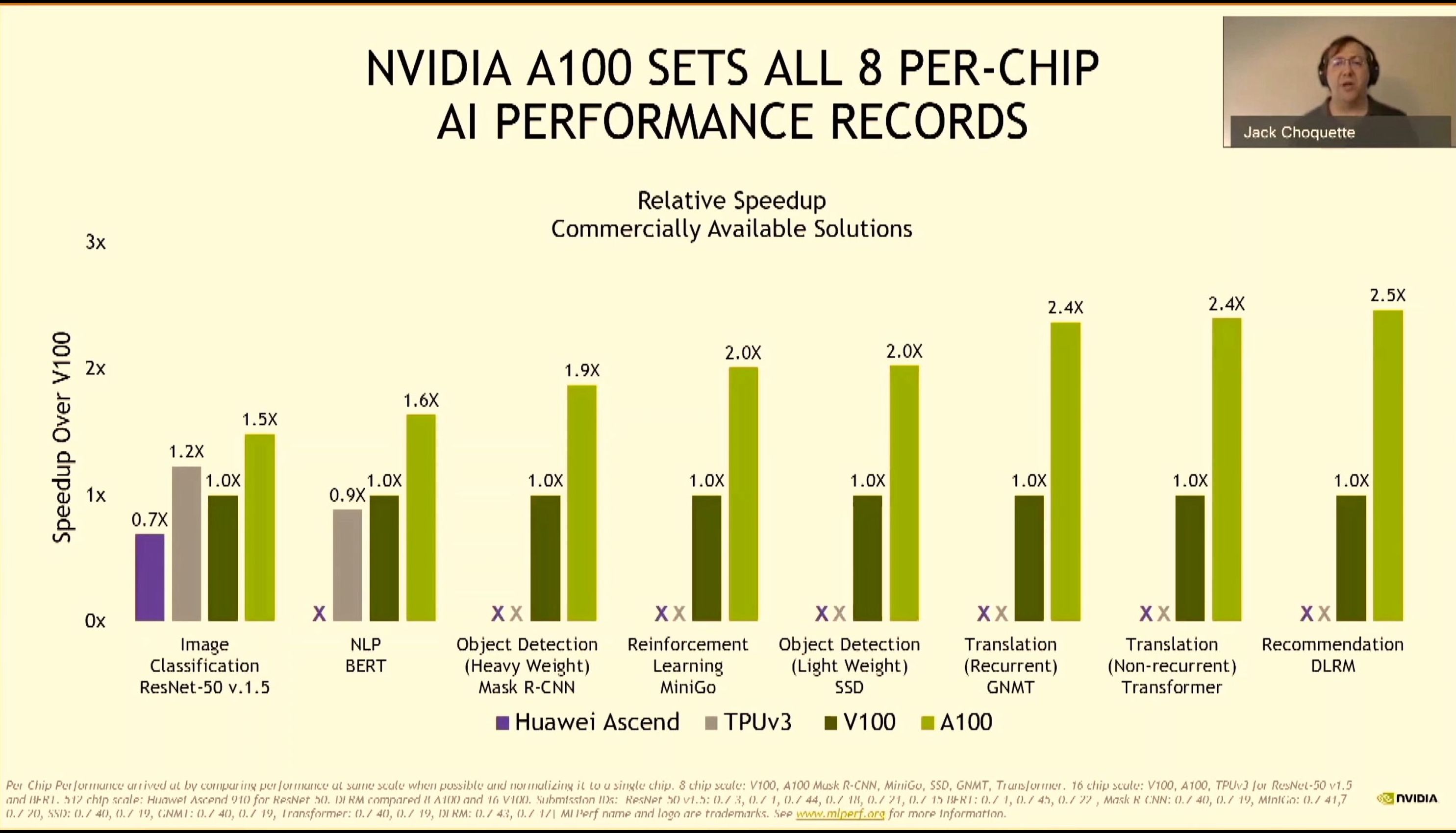
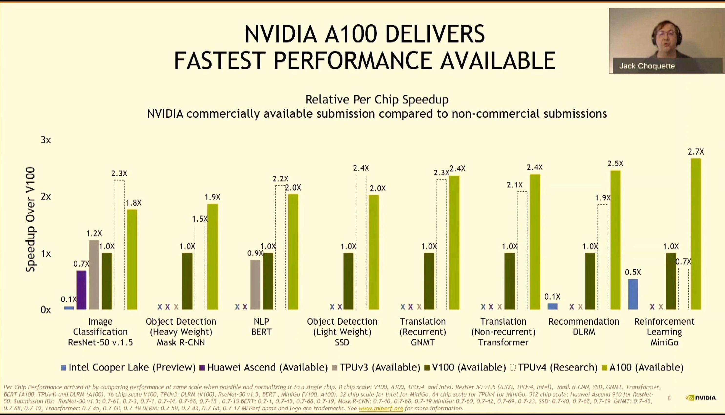
08:06PM EDT - Even wins against unreleased chips
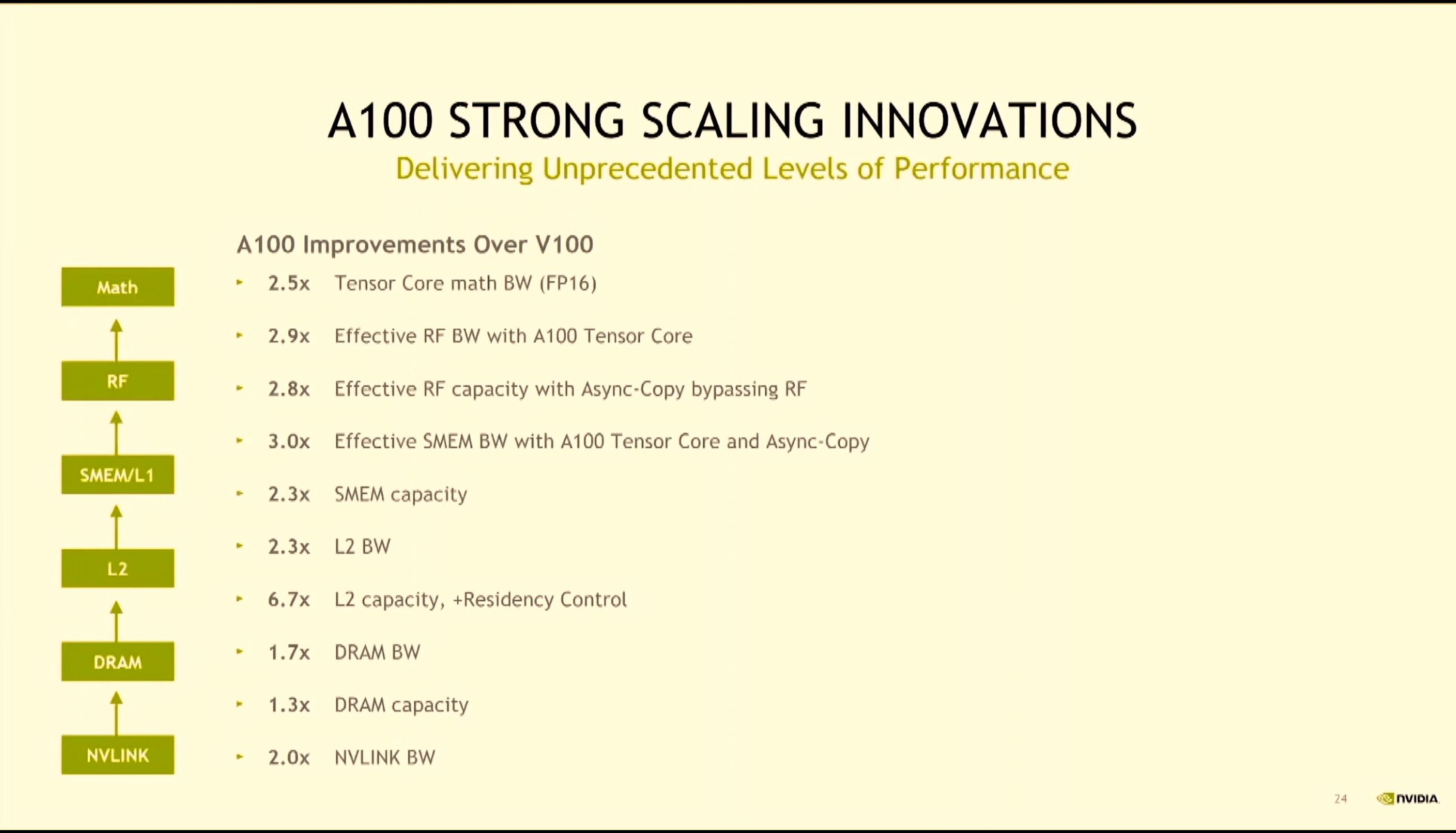
08:07PM EDT - Strong scaling
08:07PM EDT - DL strong scaling
08:08PM EDT - each layer is parallelised - A100 is 2.5x for dense FP16
08:08PM EDT - A100 targeted strong scaling
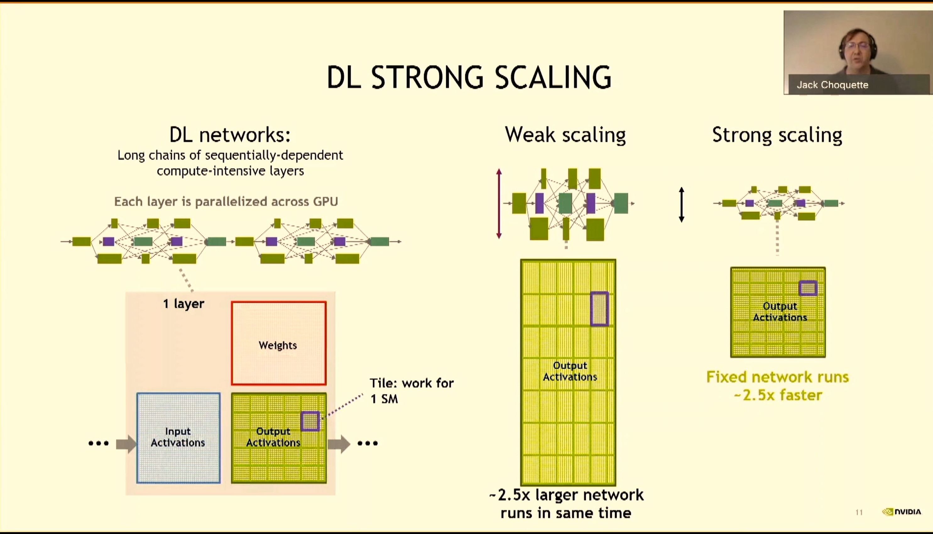
08:08PM EDT - fixed size networks
08:09PM EDT - Tensor core supports more data types
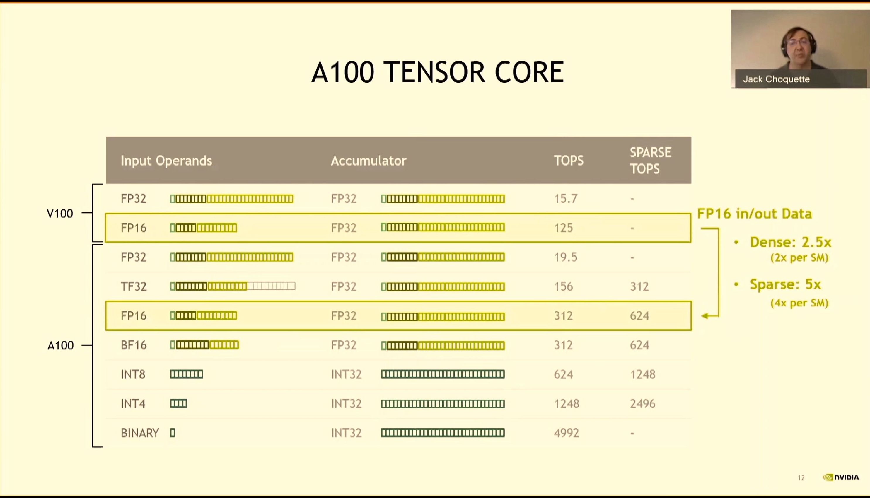
08:09PM EDT - FP32 now uses TF32 OPs, supports 20x improvement for sparse data
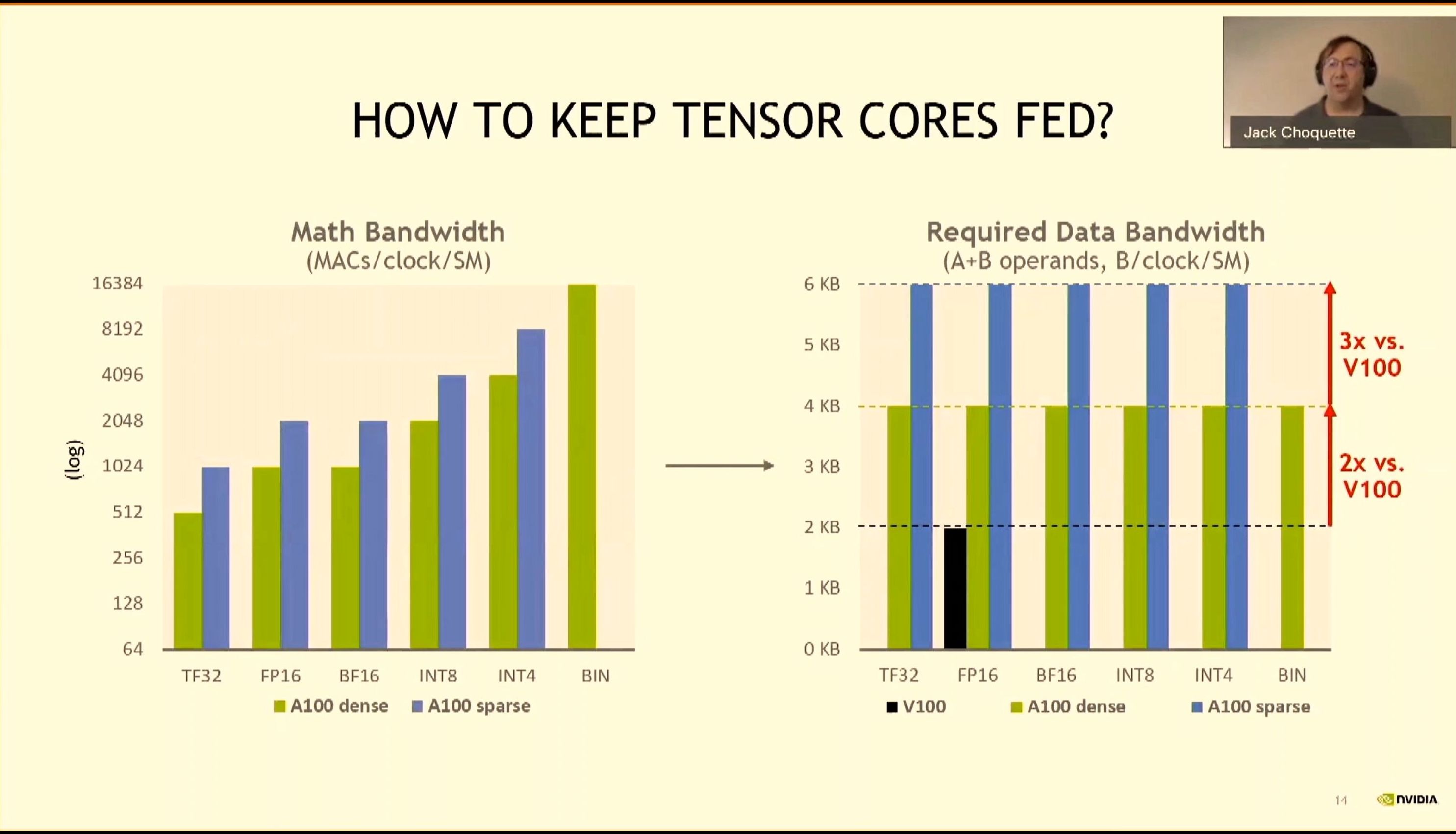
08:10PM EDT - Increase A100 data bandwidth increases based on algorithm requirements
08:10PM EDT - 6K bytes per clock per SM for sparse
08:10PM EDT - Improved speeds and feeds, and efficiency
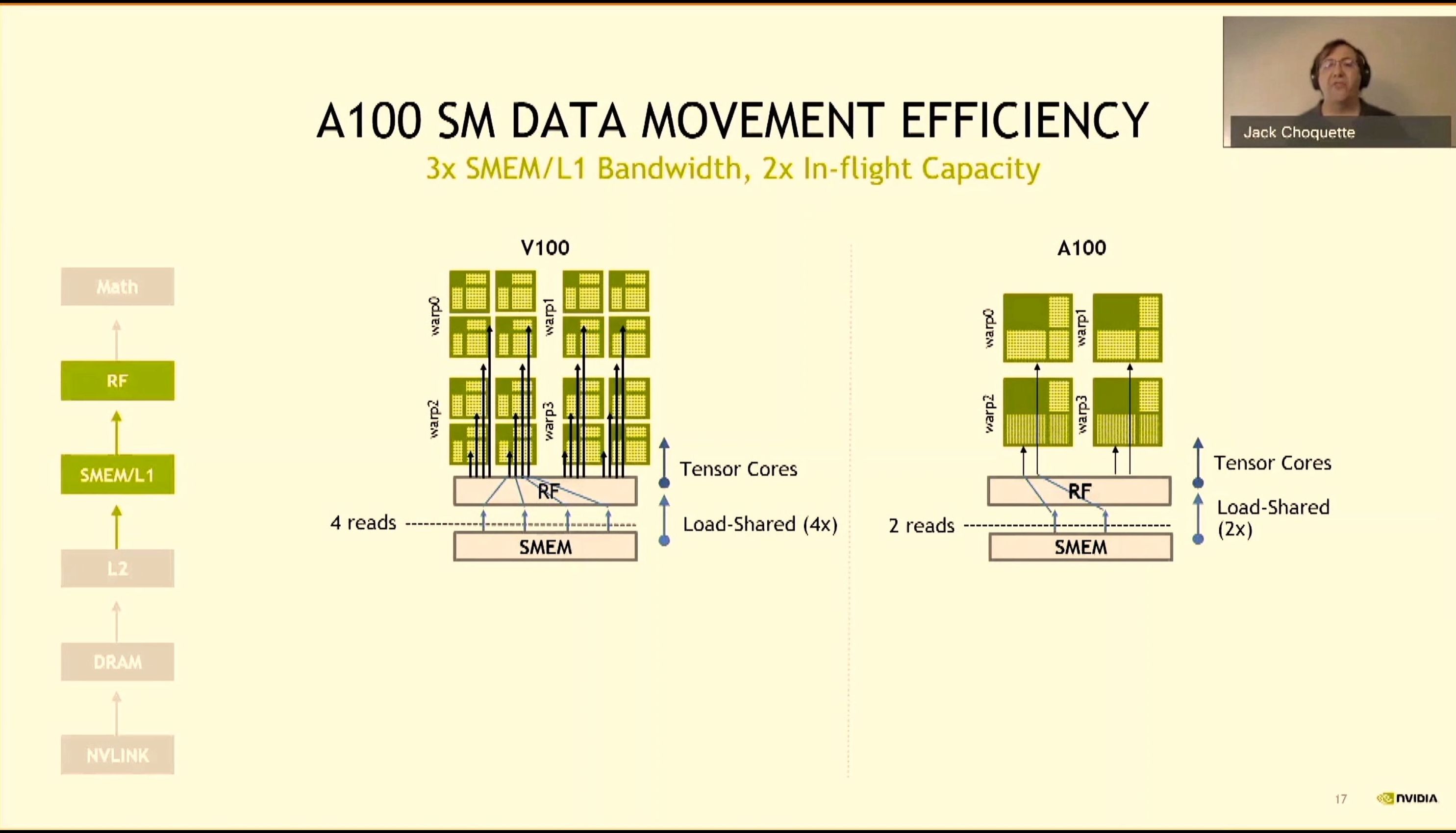
08:11PM EDT - A100 uses 32-thread tensor cores to reduce instructions required

08:11PM EDT - New load-global-store-shared copy bypassing the register file
08:11PM EDT - 3x in L1 BW, 2x inflight cap
08:11PM EDT - 2x efficiency
08:12PM EDT - Continually stream data improving utilization
08:13PM EDT - A100 couldn't just scale up V100 - L2 memory bandwidth wouldn't keep up
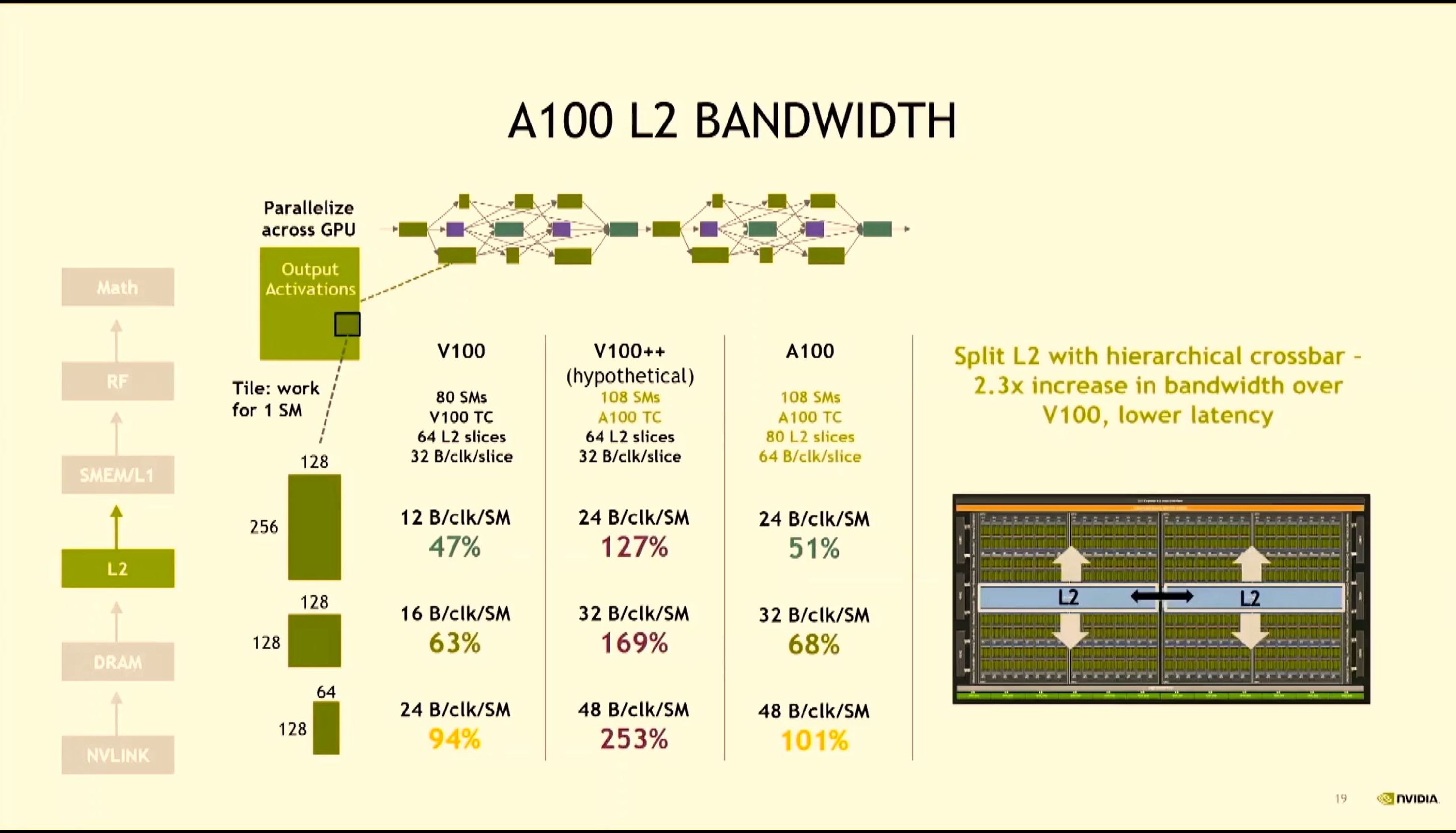
08:13PM EDT - New split L2 with crossbar - 2.3x increase in BW over V100
08:14PM EDT - Keep data near to the SM, reducing latency to L2

08:14PM EDT - Data-reuse is vital to keep utilization high
08:14PM EDT - 11x FP16 over V100 due to increased buffer support
08:14PM EDT - Larger and smarter L2
08:14PM EDT - L2 supports persistent data
08:15PM EDT - Global Memory atomics
08:15PM EDT - buffer partitioning

08:15PM EDT - DRAM BW improvements, 1.7x over V100
08:15PM EDT - ECC SECDED
08:15PM EDT - 1.25x capacity over V100 at 40 GB HBM2
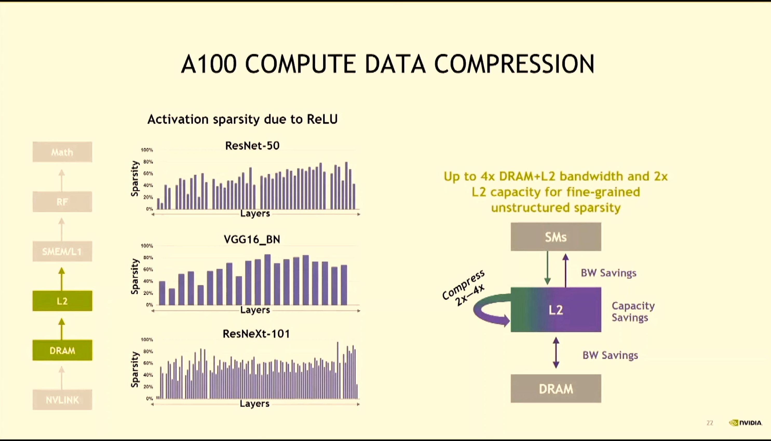
08:16PM EDT - Compute data compression within L2 cache - gives capacity savings. Saves BW, even if overall perf isn't increased

08:17PM EDT - 600 GB/s NVLink, 12x 25GB links per GPU
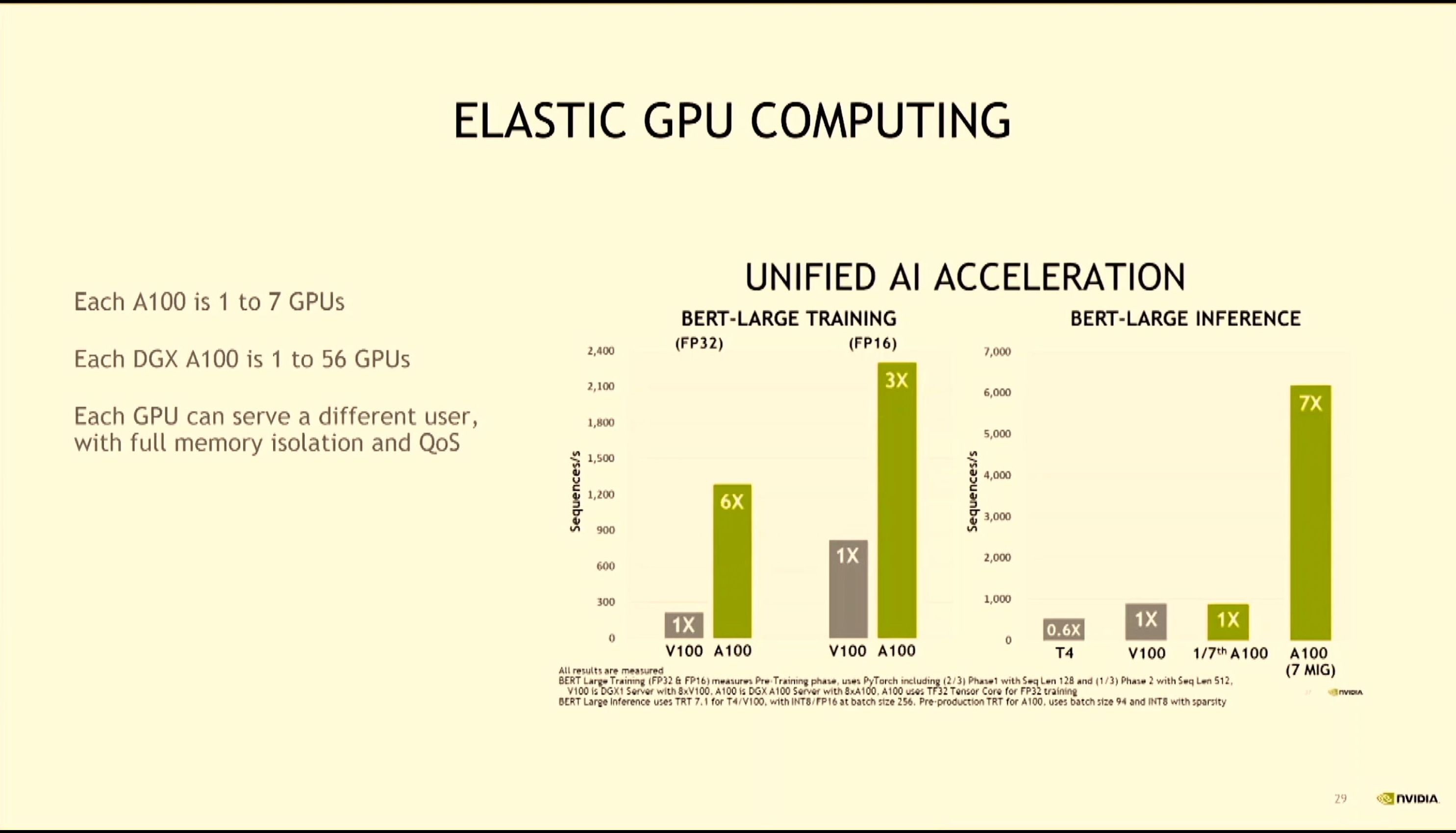
08:17PM EDT - 2-3x in raw AI improvements in perf
08:17PM EDT - Now elastic GPU for scale-up and scale-out

08:18PM EDT - This is the DGX100 - 8 A100x and 2 Rome CPUs
08:18PM EDT - NVSwitch and PEX Switches with 200G NICs
08:18PM EDT - Scalable across multiple DGX systems
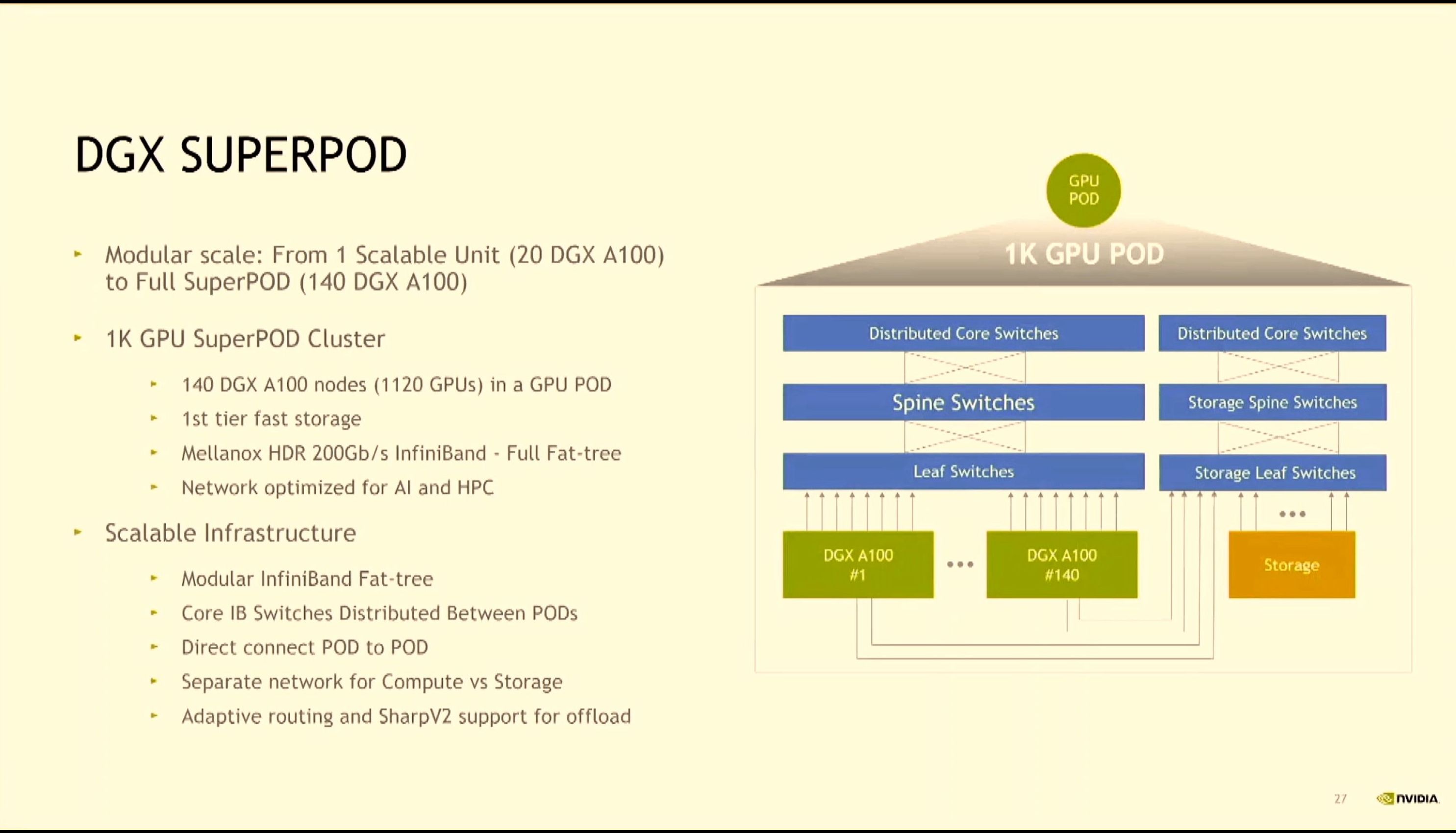
08:19PM EDT - Superpod is leaf-and-spine, for 1K GPU Pod (20 DGX100s)
08:19PM EDT - 140* DGX 100 nodes
08:19PM EDT - Separate network for storage
08:19PM EDT - modularity design allows for power distribution
08:19PM EDT - New Multi-instance GPU
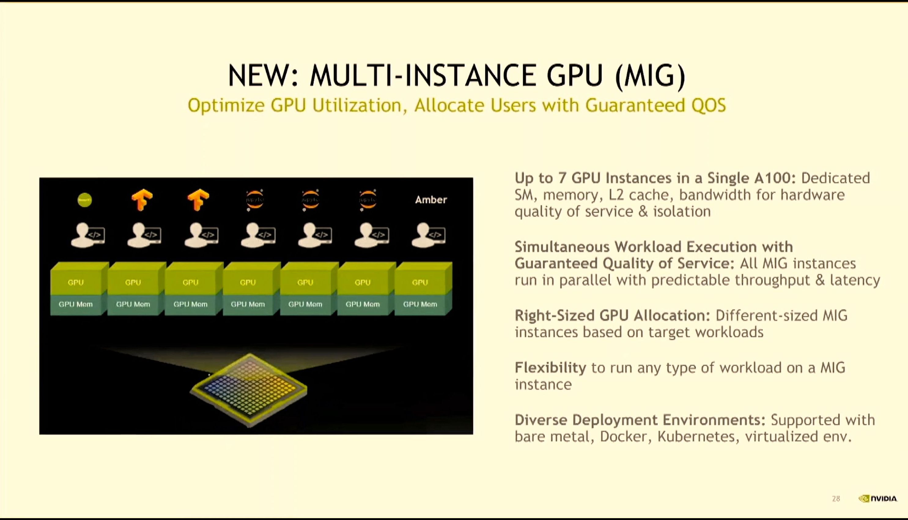
08:20PM EDT - Allows 7 GPU instances on a single A100 for better utilization
08:20PM EDT - Ian: 'Why use 25 T4 GPUs when one A100 will do?'
08:20PM EDT - Allows multiple clients per GPU in training or inference
08:21PM EDT - Full QoS support in mutli-user environment
08:21PM EDT - Async programming
08:23PM EDT - Programming models help remove complexity from developers and increase ease of use as well as performance
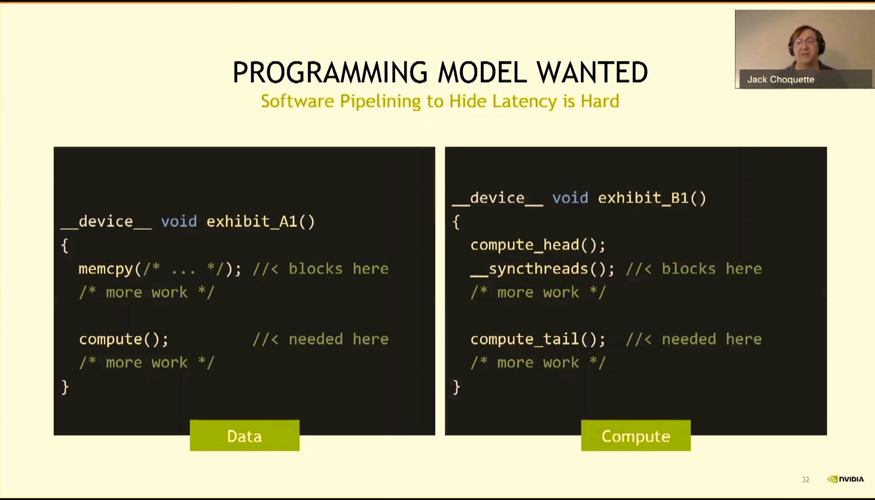
08:23PM EDT - You want to always be copying data and using data simultaneously
08:23PM EDT - But programming is inherently linear and synchronous
08:24PM EDT - New Async algorithms
08:24PM EDT - ISO C++20 barrier

08:24PM EDT - non-blocking barrier
08:25PM EDT - async data movement

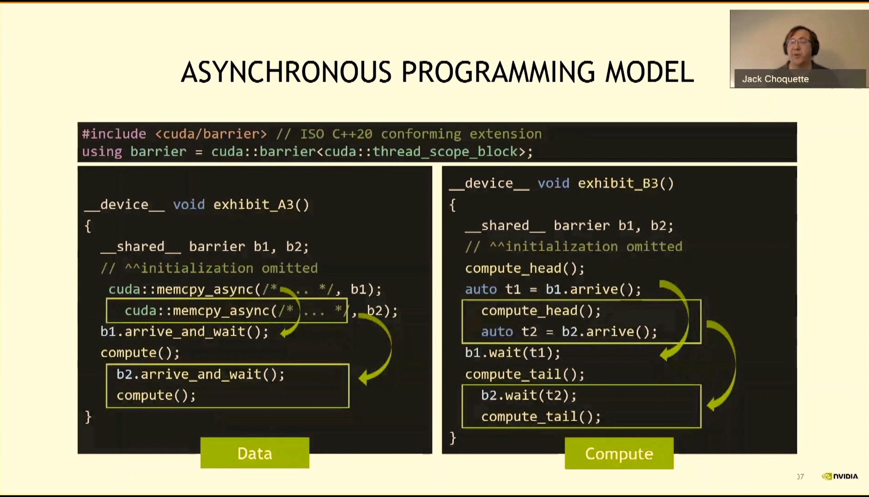
08:26PM EDT - split and arrive
08:26PM EDT - difficulty is sustaining the throughput
08:27PM EDT - creating double buffer data and compute pipeline

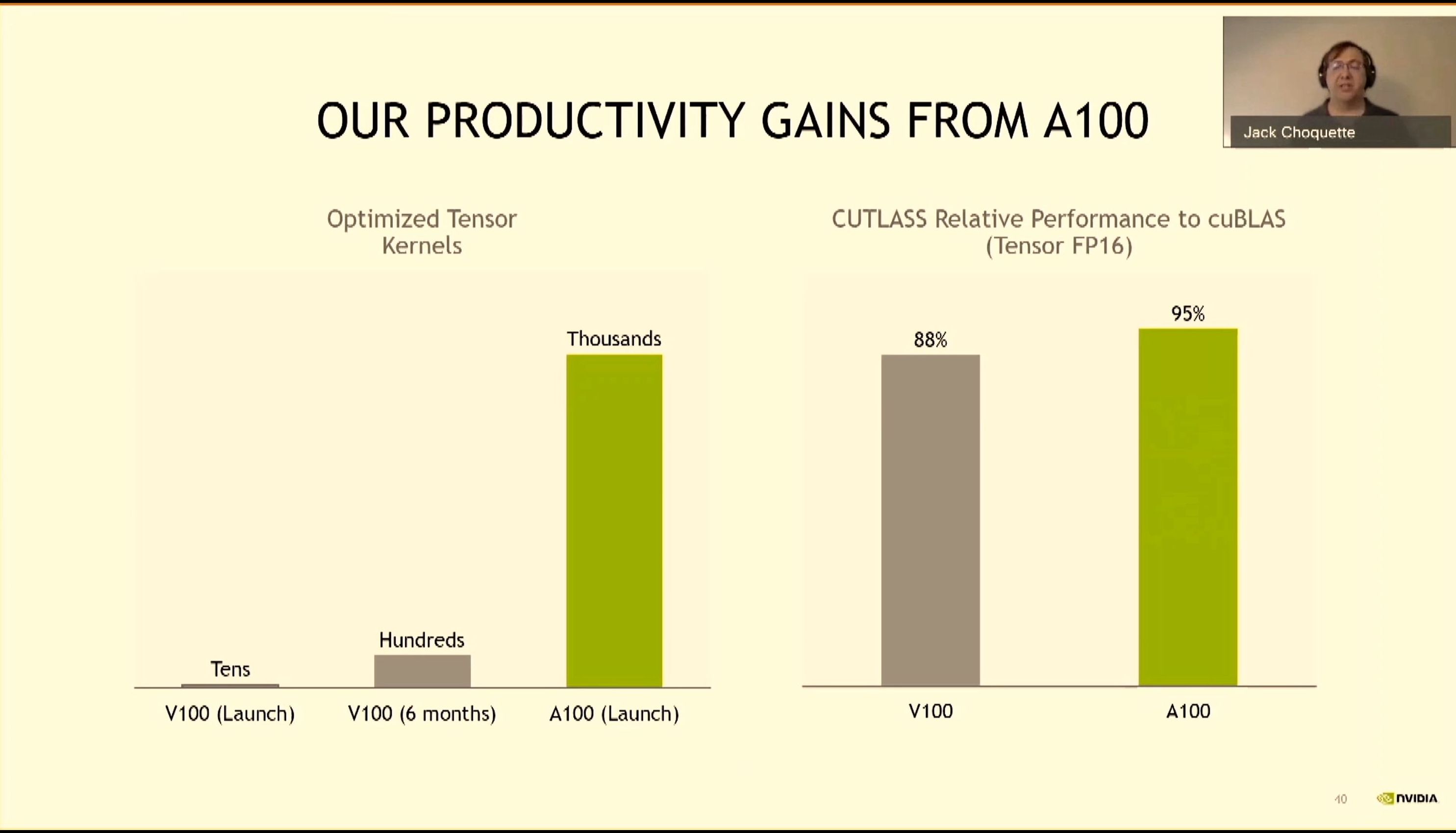
08:27PM EDT - Vast library of kernels already optimized for A100
08:29PM EDT - Q&A time
08:30PM EDT - Q: What voltage does A100 use? A: Not sure what shipping voltage is, might be in the whitepaper
08:31PM EDT - Q: Split L2 with crossbar - does this introduce latency variation? A: It doesn't, but it does equalizes of all the split areas due to data locality. L2 hits ends up with less latency variation
08:32PM EDT - Q: What improvements does the cache bring? A: Application dependent - some large, some small. The BW helps as it is a lot higher on a L2 hit, and latency is also decreased due to the design. We have benchmarks that shows both, A100 vs V100
08:32PM EDT - A: module is 48V from earlier
08:33PM EDT - Q: Would a large L3 help? A: We have, it's a trade off between capacity and the BW from DRAM. We have found it more beneficial to have a larger L2 and then the remaining requests to go to DRAM. L3 adds another layer of hierarchy - if it didn't get enough hits it would consume abnormally more power
08:34PM EDT - Q: Where does the compression happen? What type? A: It happens at the L2 - the data gets written to L2, and as evictions happen, we recompress back into the L2. We have multiple types of compression for different types of data, such as dense vs sparse techniques.
08:35PM EDT - Q: NVLink CPU to GPU? A: The systems we have announced are what they are. Not going to comment on anything that might be possible in future.
08:36PM EDT - Q: Advantage of TF32 vs BF16? A: TF32 operates on FP32 and take FP32 inputs processing with almost no accuracy loss. Better than just taking FP32 and trucating to FP16. It assists TF32 to FP16 conversion due to matissa lengths.
08:36PM EDT - End of talk - next talk is Intel Xe!


7 Comments
View All Comments
darealist - Monday, August 17, 2020 - link
AMSLOWeek2121 - Tuesday, August 18, 2020 - link
“ Q: NVLink CPU to GPU? A: The systems we have announced are what they are. Not going to comment on anything that might be possible in future.“Translation: there is a project in the works. Probably an NVIDIA ARM CPU.
Eliadbu - Tuesday, August 18, 2020 - link
I think there is already something like that with IBM POWER CPUs and Nvidia GPUs in Sierra and Summit super computers.Farwalker2u - Wednesday, August 19, 2020 - link
Seeing this article about a graphics card with around 55 billion at 7nm transistors made me think back.I pulled an ATI Radeon 9700 out of a box to look at it. In 2002 it was a pretty good graphics card. 128 MB of ram, with a bit over 100 million 150nm transistors. We have come a long way.
alfonsovazquez141 - Thursday, August 20, 2020 - link
If you are having problems in your marriage or relationship visit Lord Zakuza now via WhatsApp on +1 740-573-9483 and i assure you that things will turn around for your good. I'm happy today with my wife because of him.EditB - Monday, August 31, 2020 - link
Gillar du att spela online slots? I så fall följer du länken https://casinonsvenska.eu/free-spins-utan-insattni... Du kommer att ha det bra här.Open MKV Files - Saturday, October 3, 2020 - link
Leran how to open MKV files herehttps://openmkvfiles.com/
https://openmkvfiles.com/
https://openmkvfiles.com/
https://openmkvfiles.com/
https://openmkvfiles.com/
https://openmkvfiles.com/